Carmen Palacios-Berraquero (c2013) was a key part of a team that designed a method for creating arrays of hundreds of quantum emitters. Carmen is the lead author on a Nature Communications paper published by the team in May 2017†. Carmen is now the CEO of a spinout company nuQuantum which is commercialising some of this technology.
Previously quantum emitters were usually produced in low densities and were randomly distributed, which made it difficult to study their characteristics systematically or to improve their quality. The quantum emitters or quantum dots fabricated by the team were found to be single-photon sources in a range of wavelengths in the visible spectrum. The rest of the team consisted of researchers from the groups of Prof. Mete Atatüre and Prof. Andrea Ferrari in Cambridge, and Prof. Marco Loncar from Harvard.
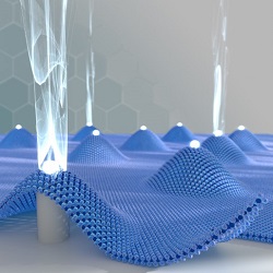
A monolayer of tungsten diselenide or tungsten disulphide was laid over a silica substrate nanopatterned with pillars (diameter of 150 nm, height between 60 – 190 nm) like a carpet. Quantum emitters were created at positions where the monolayer carpet was supported by a pillar. Atomic force microscopy and optical microscopy confirmed that presence of the monolayer carpet on the silica substrate, and photoluminescence measurements showed the locations of quantum emitters and identified the range of wavelengths emitted by each quantum emitter, as well as performing the quantum optics measurements to confirm singe-photon emission.
The team found that the height and geometry of the nanopillars influenced the emission properties of the quantum emitters, hence it may be possible to tune the emission properties of the emitters through the design of the underlying pillars in the future. Moreover, this technique of producing quantum emitters should not only be limited to tungsten diselenide or disulphide, but also other semiconducting layered materials.
The method has the potential to result in hybrid photonic and electronic structures, and could be used for applications that require accurate and precise positioning of emitters, such as optical waveguides. It has the benefits of being easily scalable and compatible with silicon chip technology.
† Palacios-Berraquero, C. et al. Large-scale quantum-emitter arrays in atomically thin semiconductors. Nat. Commun. 8, 15093 doi: 10.1038/ncomms15093 (2017)