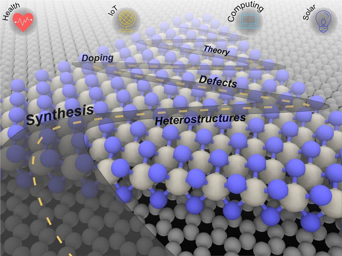
Is this world flat? For us, it’s certainly not! For some materials, however, the world is flat. The discovery of graphene made human beings, the three-dimensional (3D) creatures, realise that materials can exist in the two-dimensional (2D) world, a world where materials can be only one- or few-atoms thick. People also realised that graphene is not alone in the 2D world. Instead, it has a lot of friends, such as hexagonal boron nitride (h-BN), black phosphorous (BP), transition metal dichalcogenides (TMDs), and so on, and the list is still growing! Although these materials can be very different in properties, they have one thing in common, that is they do not naturally exist in our 3D world, and we need to put some effort to obtain them.
But why do our humans want the materials to go into the 2D world so much? The reason is that the 2D world not only makes those materials look cool, but also renders them some ‘superpowers’. In the 2D world, electrons can move like a flash, metals can become semi-conductors, things that cannot shine in the 3D world can emit dazzling light, and things that can be seen in the 3D world can be invisible in the magic 2D world. The materials themselves may not be too excited about their superpowers (or maybe I’m wrong), but humans are. Humans in the 3D world are now trying to use 2D materials to make high-performance and high-efficiency electronics and photonics, and to realise more functions that cannot be achieved before.
However, there is a big stumbling block. That is, people cannot make large-scale high-quality 2D materials, especially TMDs and TMOs, which are critical to electronics. The reason is simple, we don’t know much about how the 2D world is created. The target of my PhD project is to use an environmental scanning electron microscope (ESEM) and other in-situ characterisation tools to study how a flat world (mainly the world of TMDs and TMOs) is created. ESEM uses an electron beam to scan across the sample surface while in a gaseous environment. The electron beam helps us to see features of only few nanometres, and the ability of operating in gaseous environment enables us to observe our materials while they are growing, for example, through chemical vapour deposition (CVD) or atomic layer deposition (ALD).
Once we figure out the principles of making a flat world, we can then use the ‘bottom-up’ methods to fabricate it easily, and make our life to be gifted by it.
NanoDTC PhD Student, c2020