Gallium nitride (GaN) based semiconductors, perhaps the most important semiconducting materials family since silicon, has revolutionized the electronics industry. These can emit a bright blue light for only a small amount of current that is passed through it. This has positioned GaN-based semiconductors as the material of choice for the manufacture of power saving white light-emitting diodes (LEDs). GaN also possesses phenomenal electronic properties that make it attractive for use in high electron mobility transistors. These are applied in technologies which require high-gain and low noise such as radio telescopes.
To further improve the capabilities of GaN-based electronic devices and those of other technologically important semiconductors, it is crucial that we understand the underlying physics and phenomena that govern their properties. One such consideration is that of the charge carrier dynamics. Charge carriers are particles, for the case of electrons, or quasi-particles, for the case of holes, that carry electrostatic charge within materials such as semiconductors. Their lifetimes, the period between carrier generation (birth) and carrier annihilation (death) can reveal valuable information about the semiconductor. However, for GaN, the magnitude of this quantity is usually in the nanosecond (10-9) and picosecond (10-12) regimes and is thus challenging to measure.
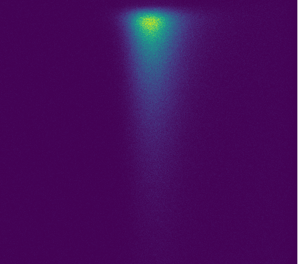
My research focuses on cathodoluminescence hyperspectral imaging. This technique utilises a focused electron beam that imparts energy into the material of interest allowing it to emit light that is then collected, separated, and analysed. For the purposes of investigating carrier dynamics in semiconductors the electron beam is pulsed by striking the electron source with a pulsed laser beam. This allows us to gain temporal or time-resolved data-sets with a resolution in picoseconds (10-12) allowing lifetime measurements to be performed. More importantly, the use of a focused electron beam provides the capability to probe different nanoscale regions on the surface of the sample allowing comparisons between structural properties and carrier dynamics to be made.
NanoDTC Associate, a2020