Plastic semiconductors as an alternative to silicon
When we think of electronics, what usually springs to mind is a black box of metal and silicon. The advent of the laptop and more recently the tablet computer has reduced the size of these boxes, but they remain the same in most respects. Over the last few decades, an increasing amount of research has focused on plastics that can, like silicon, function as semiconductors. Because these materials are inherently flexible, entirely new possibilities emerge: tents with built-in solar panels to provide a mobile power source, clothes with integrated electronics or devices produced extremely quickly by printing the circuitry just like a newspaper.
Ideally we would like to be able to predict the performance of a material based on nothing besides its chemical structure, but the complexity of these materials makes this very difficult. Many years of research has provided plenty of information on various approaches that “should work”. New materials are made and tested in a trial and error process drawing on expertise from both chemistry and physics.
My work focuses on testing new materials using many different techniques to examine their physical, optical and electrical properties. When a particular material shows good electrical performance, we take note of its other properties and use that knowledge to guide the synthesis of the next material. Alongside that we spend a lot of time experimenting with different ways of processing materials. In particular, I work with spin coating, which spins a droplet with material dissolved in it at high speeds to form a well-ordered thin film on a surface, and zone casting, a novel method that involves dragging a droplet across a surface to deposit the dissolved material. Zone casting has the advantage of pulling the molecules in the solution in one direction, which can produce very highly ordered structures.
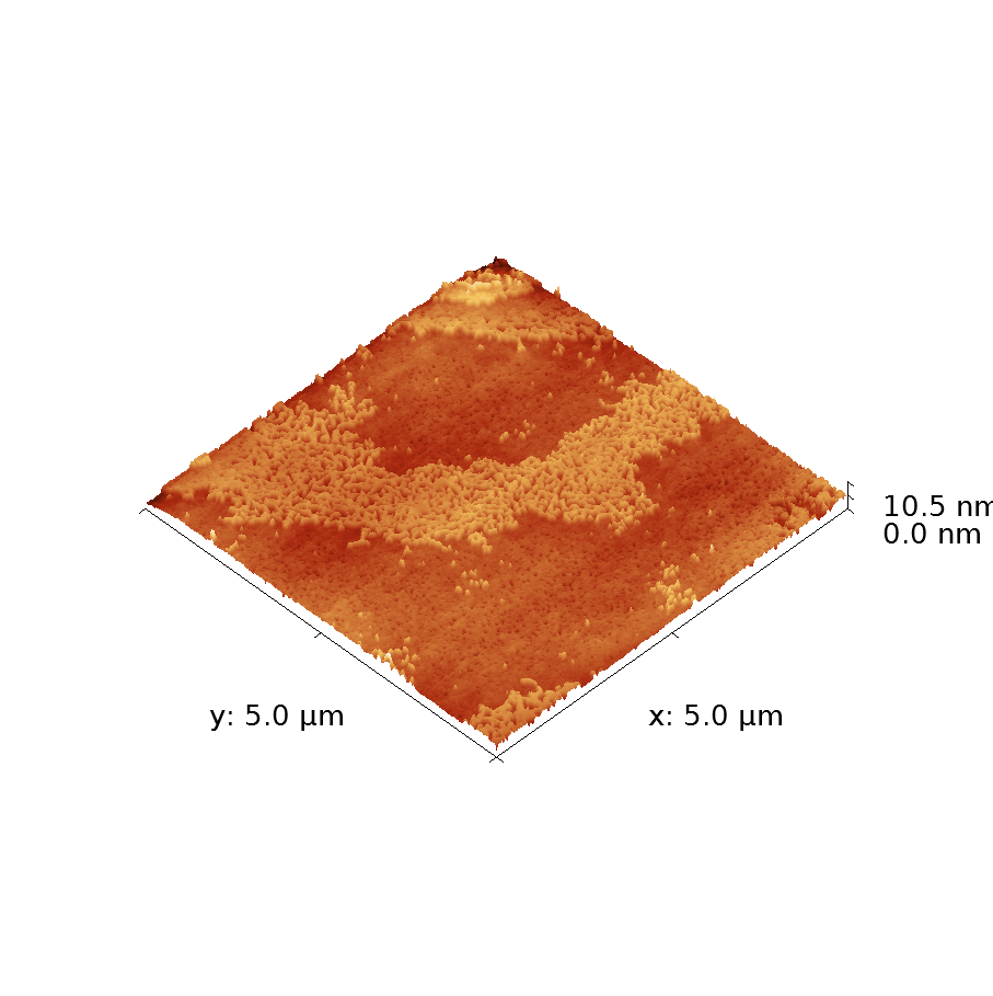
One example of this is a material commonly called PBTTT (it has a real name, but it’s far too long and boring to reproduce here. Unless you’re really curious. ), which showed good electrical properties for its time. In this case chemists developing the material had learned that materials that form large crystals often had good conductivity: the well-ordered structure of a crystal removes many “charge traps” which can hamper electrical performance. PBTTT forms large crystal structures in a distinctive terraced formation (Figure).
This image was produced using atomic force microscopy (more commonly known as AFM). For such a fancy name, the technique is actually very simple: a tiny needle at the end of a bendy rod is dragged gently across the surface. The microscope tracks the motion of the needle as it follows the contours of the surface and builds up a picture using that data. This particular image is 5×5 micrometres in size which, while small in everyday terms, is a relatively large size for crystal structures in such a material. The vertical scale is even smaller than the horizontal; each step is only 2 nanometres high. To give that some context, a human hair on this scale would be 10,000 times larger than this image. You’d probably need a larger monitor to view that.
Fortunately, you can already get some very large displays made from organic semiconductors.
More recently, we’ve been testing a set of materials that are very similar to a widely studied group, the polythiophenes. By changing just one atom in the structure, we aim to coax the material to form a better-ordered structure. Results are still coming in, but early device tests have shown improved electrical performance in the new materials, which is of course encouraging.
I work with the Optoelectronics Group at the Cavendish Laboratory, and with members of the Nanostructured Materials and Devices Group at Imperial College London.