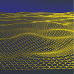
Graphene is a two-dimensional material consisting of a single layer of carbon atoms arranged in a honeycomb structure. It is now at the centre of an ever growing research effort owing to its unique properties which are interesting for both fundamental science and applications. Graphene development could impact products in many industries, from flexible, wearable and transparent electronics, to high performance computing and spintronics.


My project combines the field of graphene and two-dimensional materials with the field of plasmonics, another widely studied topic in current research. The combination of these two fields shows great promise for developments within the area of photodetectors. Graphene has a range of properties that are advantageous for photodetection.
Whereas most conventional semiconductors are optically active within a narrow range of wavelengths, graphene is active within an unprecedented wavelength range from the visible to the infrared. In addition, its electronic properties allow the realisation of very high photodetection speeds. However, these incredible optical properties come at a price as graphene is only one atom thick, so its overall absorption is low. The field of plasmonics is based on using collective oscillations of electrons in metals to enhance the interaction between light and matter, and thus graphene and plasmonics naturally complement each other in the area of photodetection and photovoltage generation.
![Single-layer graphene (SLG) and bilayer graphene (2LG) sandwiched between a flat gold layer and a layer of gold (Au) nanoparticles. We use this robust nanoparticle-on-layered-material configuration as a versatile platform to investigate a wide variety of plasmonic and monolayer functionalities and devices [Mertens et al., Nano Lett., 2013]](https://www.nanodtc.cam.ac.uk/about-the-nanodtc/c2010-research/electricityfromgraphene4.png)
Cambridge Graphene Centre – http://www.graphene.cam.ac.uk/
Nanophotonics Centre – http://www.np.phy.cam.ac.uk/