Since the Copernican model of the solar system we have known that the earth revolves around the sun. Efficiently harvesting sunlight will also be at the centre of our solution to the current global climate emergency.
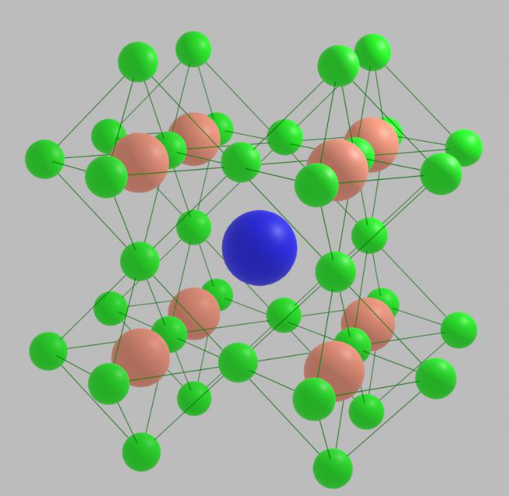
The Sun potentially represents a huge clean energy source, with approximately 120 terawatts of power hitting Earth from incident solar radiation, this is 6x more than global power consumption!1 Harnessing this truly astronomical resource more efficiently will undoubtedly be part of mitigating climate change. I am particularly interested in a family of materials called metal-halide perovskites (MHPs) which are a promising candidate to form a part of next generation photovoltaics. Astonishingly single junction solar cells made from MHPs have shown efficiencies of up to 25.5% which is already very close to established silicon based technology.2 When considering MHPs are easy and cheap to produce, whilst being a relative newcomer to the field this makes their meteoric rise in performance even more impressive. However these improvements have often outpaced understanding into the nanoscale structure and there is currently a chink in the MHP’s armour due to their intrinsic instability caused by so called ‘deep trap clusters’ which limit performance and seed degradation.3
A solar cell works by using light to produce charge carriers (electrons and holes) in a material, these are then collected at separate electrodes to produce a flow of electricity. The ‘bad apple’ trap states can oppose this process by capturing the energy from the charge carriers and dissipating it as heat, something we want to avoid in high performance photovoltaics. In my work I aim to understand the nature of the trap states by using scanning electron diffraction (SED), a technique where electrons are used in a microscope instead of light. This will provide local information on impurities and defects and then by combining this with optical measurements we hope to relate structure to device performance. I am especially interested in passivation strategies, where the MHPs are chemically treated after formation and whether this can be better understood using a combination of these analytical techniques.
In my future work I aim to develop a method so that impurities and trap states can be identified using the optical features shown from photoluminescence measurements. This would allow the screening of material at large scales hopefully making MHPs a more commercially viable option for the next generation of photovoltaics.

References:
- D. J. C. MacKay, Philosophical Transactions of the Royal Society A: Mathematical, Physical and Engineering Sciences, 2013, 371, 20110431.
- T. Wu, Z. Qin, Y. Wang, Y. Wu, W. Chen, S. Zhang, M. Cai, S. Dai, J. Zhang, J. Liu, Z. Zhou, X. Liu, H. Segawa, H. Tan, Q. Tang, J. Fang, Y. Li, L. Ding, Z. Ning, Y. Qi, Y. Zhang and L. Han, Nano-Micro Letters, 2021, 13, 152.
- T. A. S. Doherty, A. J. Winchester, S. Macpherson, D. N. Johnstone, V. Pareek, E. M. Tennyson, S. Kosar, F. U. Kosasih, M. Anaya, M. Abdi-Jalebi, Z. Andaji-Garmaroudi, E. L. Wong, J. Madéo, Y.-H. Chiang, J.-S. Park, Y.-K. Jung, C. E. Petoukhoff, G. Divitini, M. K. L. Man, C. Ducati, A. Walsh, P. A. Midgley, K. M. Dani and S. D. Stranks, Nature, 2020, 580, 360–366.
NanoDTC PhD Student, c2021
