Development of tiny LED-like light sources can allow perfectly secure communications
The semiconductor Gallium Nitride (GaN) has become famous in recent years for its applications in LED lighting. Its material properties allow for high efficiency, long lasting and nicely coloured bulbs to be created. The success of these LEDs relies on very small structures (several billionths of a meter across), such that quantum mechanical effects can be utilised. These quantum effects are unlike anything which can be reproduced with larger, classical physics.
One novel use for quantum behaviour at this scale is to make the smallest possible sparkle of light, a single photon. By having regions of the semiconductor so small that only one electron can fit inside it, a ‘quantum dot’ (QD), only one optical transition can occur at a given time, so photons are emitted one-by-one


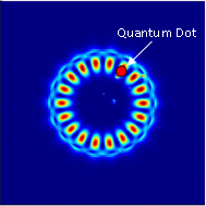
A small droplet (quantum dot) of light-generating gallium-nitride is created within a disk-shaped cavity one micron (one millionth of a meter) in diameter. Viewed schematically top-down (left) shows the optical resonances, while structure is viewed by an electron-microscope (right)
Whilst QDs have been shown to be reliable single photon sources in several materials systems (such as InGaAs), there exist fundamental limitations to these technologies. Their wavelength are ill-suited to single photon detection, attenuation through free-space is less than ideal, and sources must be kept at very low temperatures (approximately -269°C).
Gallium Nitride materials have a wider range of available electrical properties which can potentially overcome these problems. For example, operation of GaN-based QDs as single photon sources has been demonstrated up to -73°C, which is achievable with liquid nitrogen or electrical cooling and would be much cheaper to operate than those which require liquid helium.
However production of good quality GaN materials is difficult as there is a significant lattice mismatch with any material on which GaN is grown; GaN wafers typically have very high densities of defects and dislocations (>108cm-2). These dislocations reduce both the light output of the materials, reduce their robustness, and lead to shifts in the emission properties from QDs in their vicinity (known as ‘spectral diffusion’). Production of QDs is also limited by the reduced strain between the GaN and InGaN layers required, making traditional QD growth methods (Stranski-Krastanov, ‘SK’) growth difficult to achieve. Several other methods for growth of GaN/InGaN QDs have been developed [1]. My research is focused on examining the causes of drift in the emission properties of QD layers formed by a process known as ‘CVD Modified Droplet Epitaxy’ [2], as well as examining the effects of dislocation density and impurity inclusions near the QD layer. Through atomic force microscopy (AFM) and micro-photoluminescence (µPL) studies, a significant dependence of the drift in emission peak of the QDs to the dislocation density has been found, as well as significantly bad effects from impurities in the vicinity of the QDs. Furthermore PL studies on QDs placed in micro-disk cavities, which should increase their efficiency, are also being performed.
Centre for Gallium Nitride: http://www.gan.msm.cam.ac.uk/
[1] A. F. Jarjour, R. A. Oliver, and R. A. Taylor, “Nitride-based quantum dots for single photon source applications,” Physica Status Solidi (a) 206, 2510 (2009).
[2] R. A. Oliver, et al., “InGaN quantum dots grown by metalorganic vapor phase epitaxy employing a post-growth nitrogen anneal” Applied Physics Letters 83, 755 (2003).