In-situ metrology techniques are crucial in order to characterise how two-dimensional materials, such as graphene, can be grown by chemical vapour deposition. Such techniques will lead to greater understanding and control of the resulting material properties, critical for potential applications.
Imagine you are asked bake a cake for the first time – except, you aren’t given any instructions. All you are given are the ingredients and a finished cake for reference. You are missing the crucial information about how to get from the raw ingredients to the finished cake. How would you solve this problem?
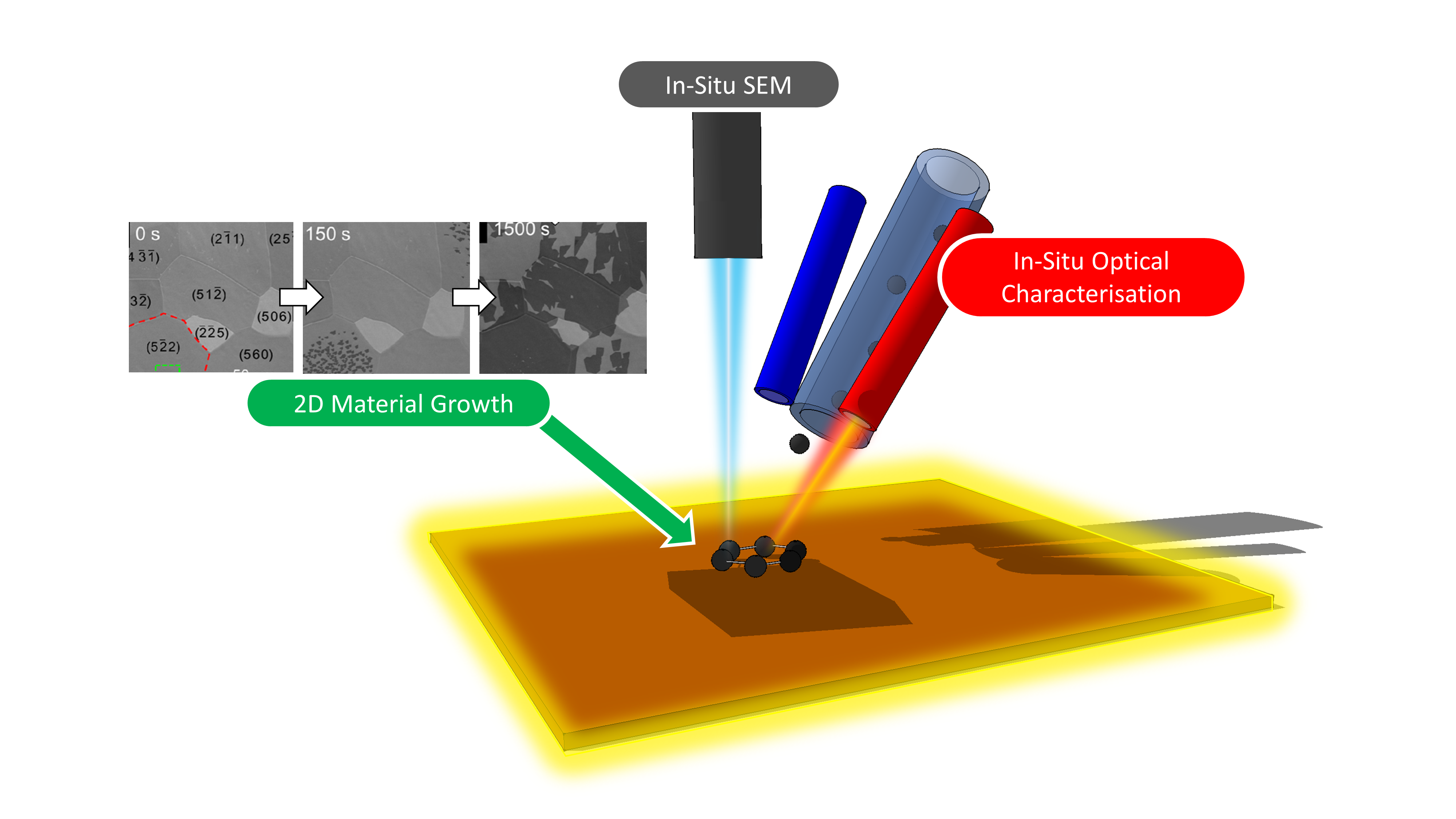
You could deduce some information from just studying the cake. You could slice it open and have a guess at some of the steps involved by looking at its internal structure, but this would only get you so far. What you really need to do is to see the cake being made. In fact, we are faced with a similar problem when making nanoscale materials, in that understanding how such materials form is challenging. However, now we have the added difficulty that the ingredients and the nanoscale materials themselves are so small that we cannot even see them with our naked eye, and we require special methods of metrology to visualise them.
In my research, I focus on how to produce a class of nanomaterial named two-dimensional (2D) materials such as graphene. These materials are useful for a variety of applications, ranging from serving as a nanoscale sieve to sense bio-molecules, to being integrated into electronic or spintronic devices. However, there are many challenges associated with such materials. One key issue is how to manufacture them in high volumes necessary for industry, whilst also ensuring sufficient quality for their intended applications. A promising approach is to “grow” them through a process known as chemical vapour deposition (CVD). Much like baking a cake, we introduce our ingredients (reactive gas molecules) over a metal catalyst at high temperatures and pressures, causing them to decompose into atoms. The resulting atoms are then able to crystallise into our material of interest. By tuning parameters such as the temperature at which they grow, gas pressure and the choice of catalyst, we are able to control the nature of the final product.

However, in order to know which parameters to tune and how to tune them, we first need to know the mechanism by which these materials grow. We need to understand the intermediate steps between the raw ingredients and the fully grown material, which brings us to our second challenge – how do we “see” such materials to begin with? We have many experimental techniques by which we can see 2D materials ex-situ, i.e. after growing them. Techniques such as scanning electron microscopy (SEM) allows us to directly image our material, while X-ray photoemission spectroscopy (XPS) and Raman spectroscopy can give us chemical and structural information. However, what we really need are modes of metrology that are in-situ and allow us to characterise the growth process in real-time. This is challenging, as CVD requires very harsh conditions that a standard characterisation equipment is not built to withstand: temperatures of up to 1000oC and very reactive gases at high pressures.
During my PhD, I am engineering a specialised SEM that is able to overcome these issues to provide in-situ imaging capabilities. The aim is to apply this technique to understand how CVD can be used to grow not just graphene but many other 2D materials such as hexagonal boron nitride and the transition metal di-chalcogenides, in a step towards the scalable manufacturing of 2D materials.
Ryo Mizuta
NanoDTC PhD Student 2016